LONGFORCE MANUFACTURING
Longforce is based in Suzhou, China, and was established in 2023. It has a workforce of 700 and covers an area of 59,090 square metres.
Before a Lexar card reaches your camera, it starts as a silicon wafer which is machined and cut into small ‘packages’ or squares. A single layer of the end product of that chip is thinner than a single hair.
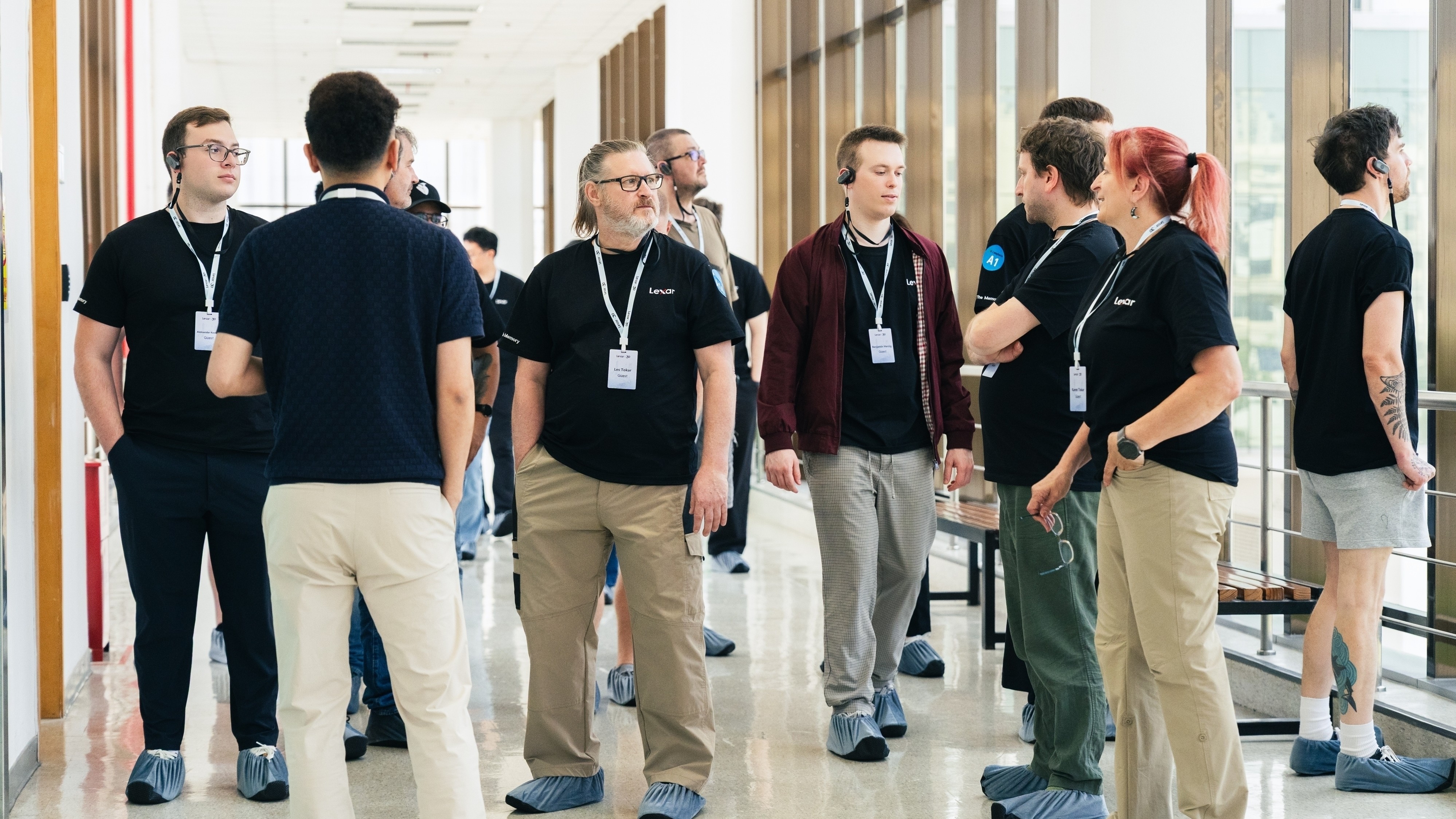
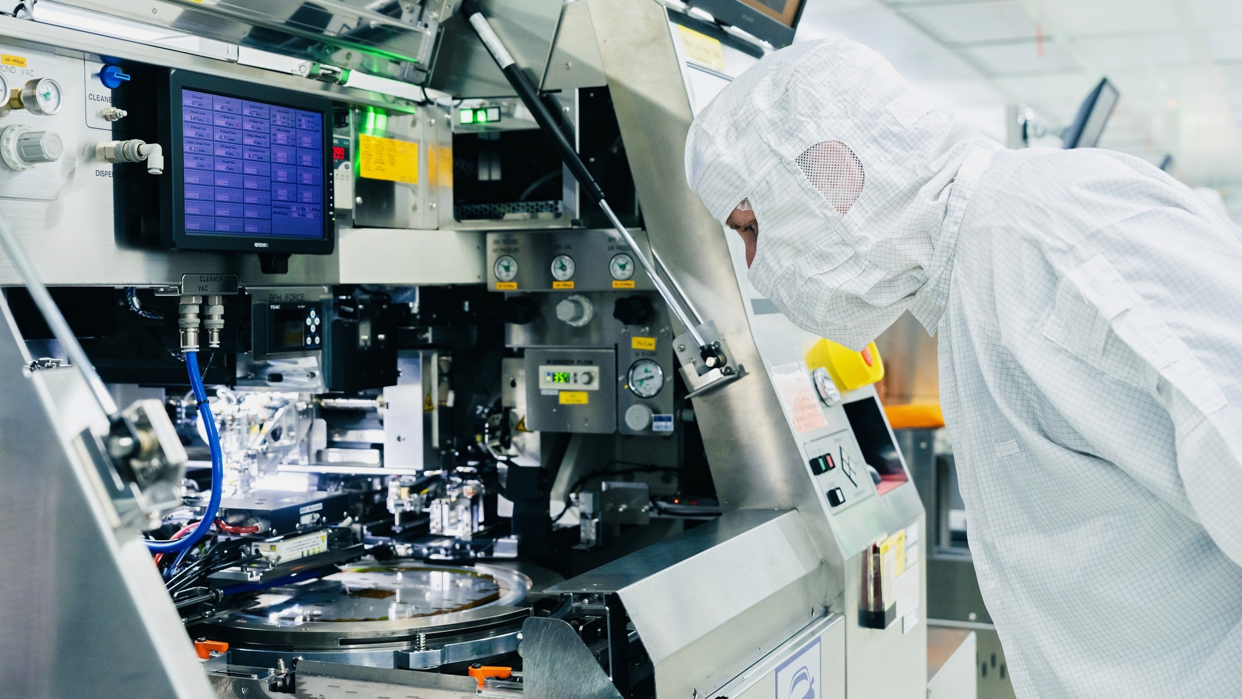
When entering the facility, cleanliness is paramount. Longforce has ‘zero-contamination’ packaging which means the environment that wafers are manufacturted and cut into chips is 99.9% dust free and sterile. For that reason, strict precautions must be taken before entering the cleanrooms.
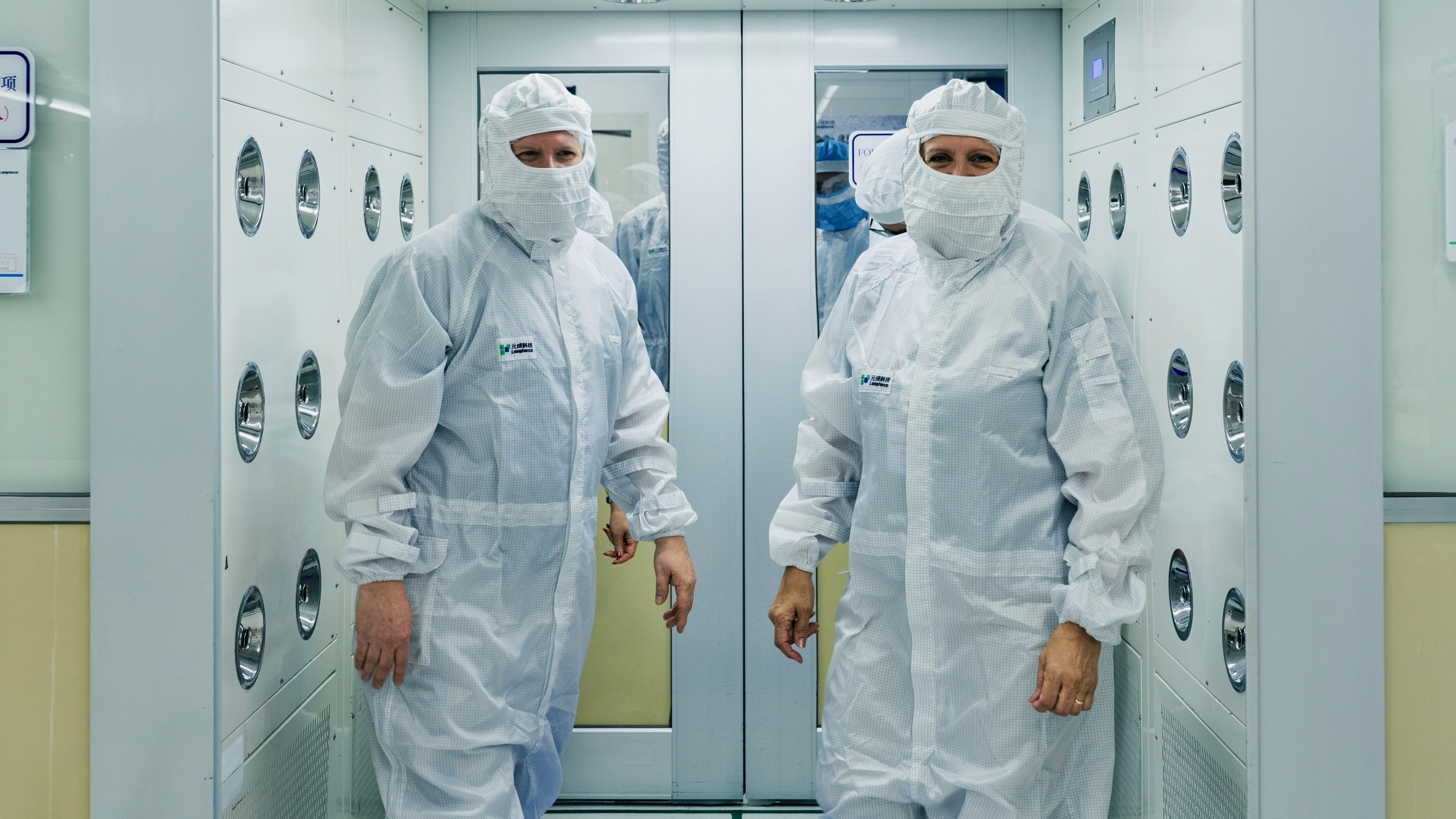
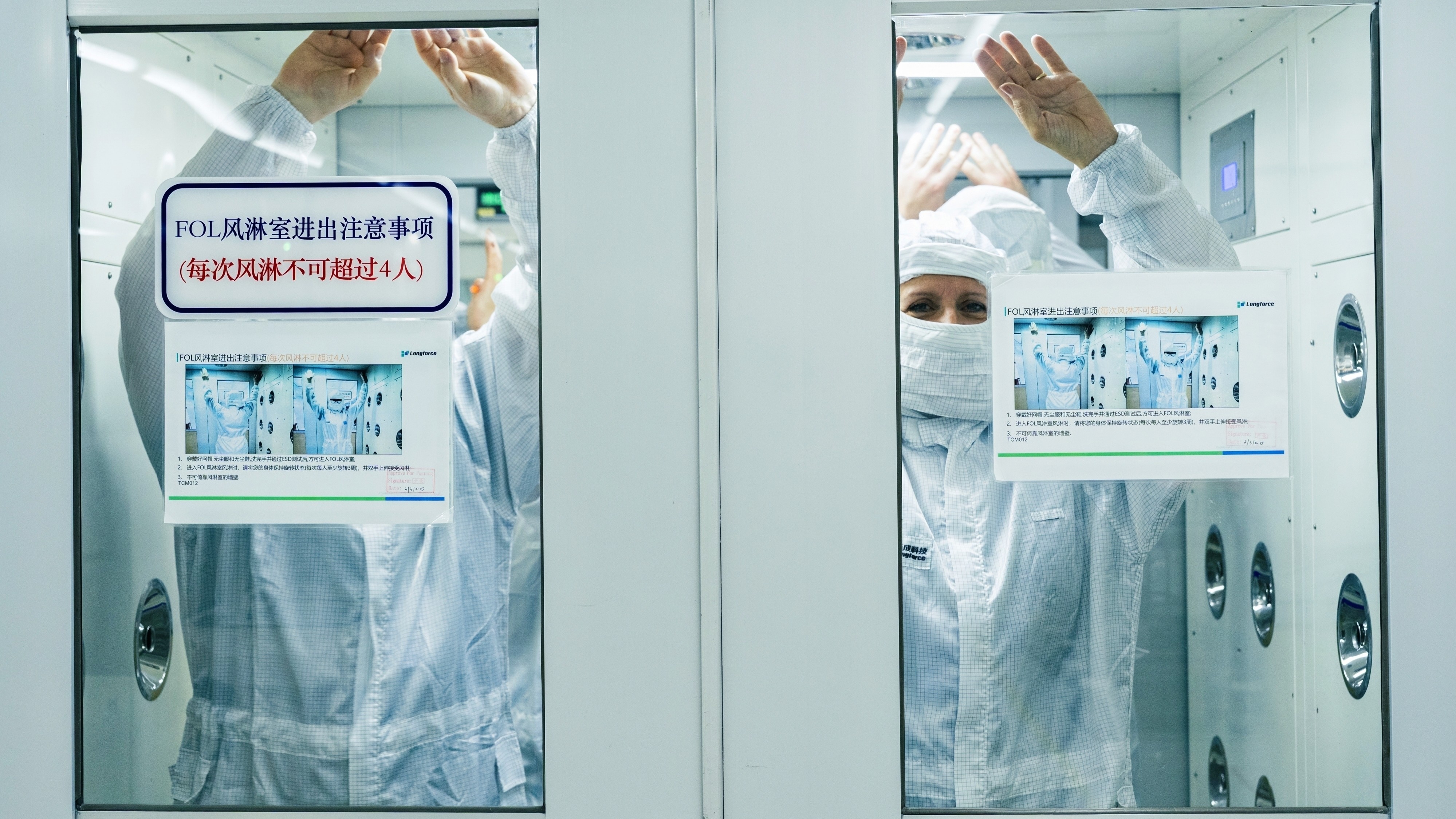
This sealed room ensures there are no duct particles on ones person whatsoever. A single particle of dust can wreak havoc to a wafer in the machining process, causing thousands of dollars in damage.
This is a silicon wafer. We have posted of these many times before on The SSD Review and I believe them to be one of the greatest technological achievements historically.
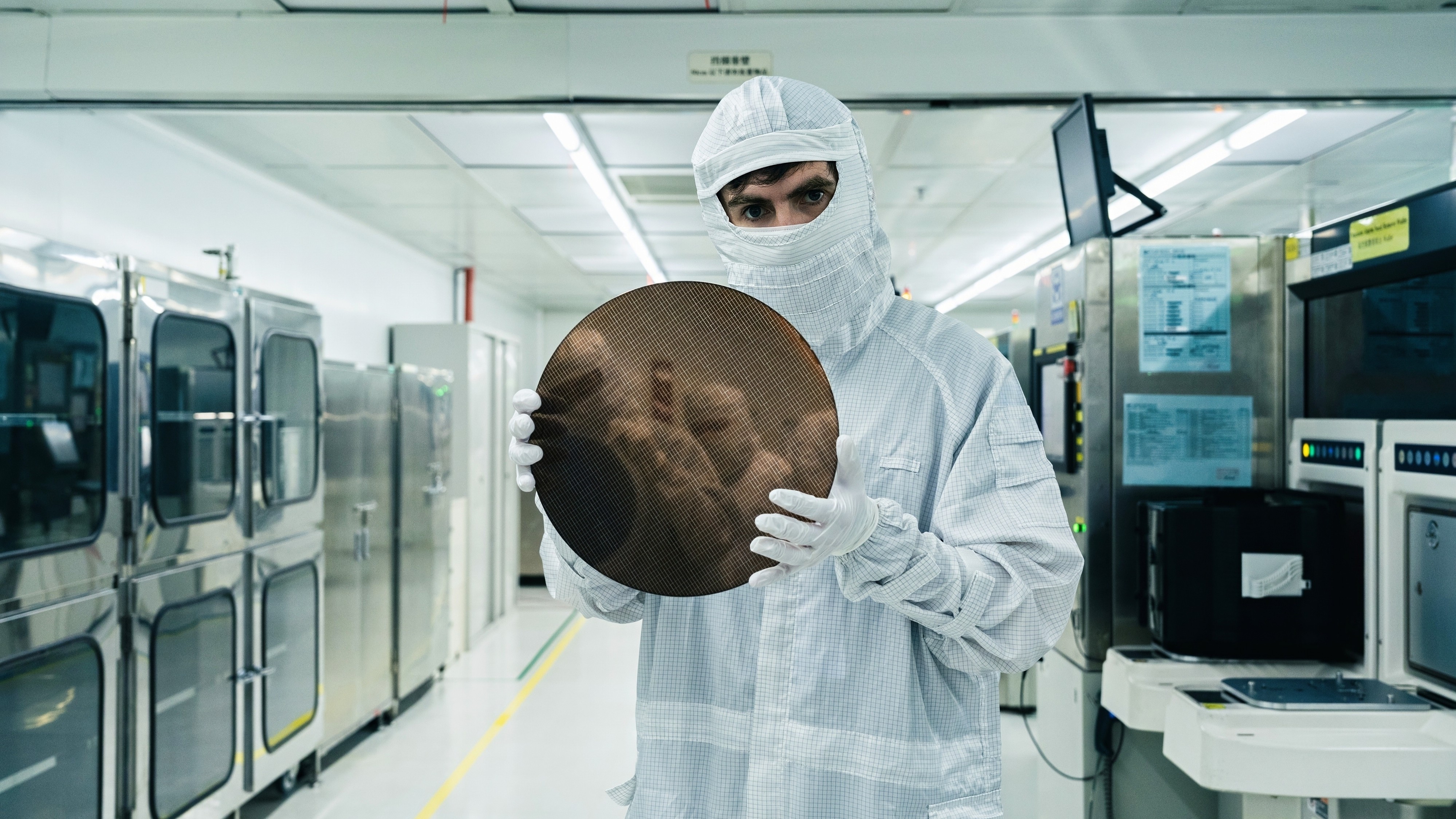
If you enlarge the photo above, you will get a closer look at how the wafer is divided and cut into chips.
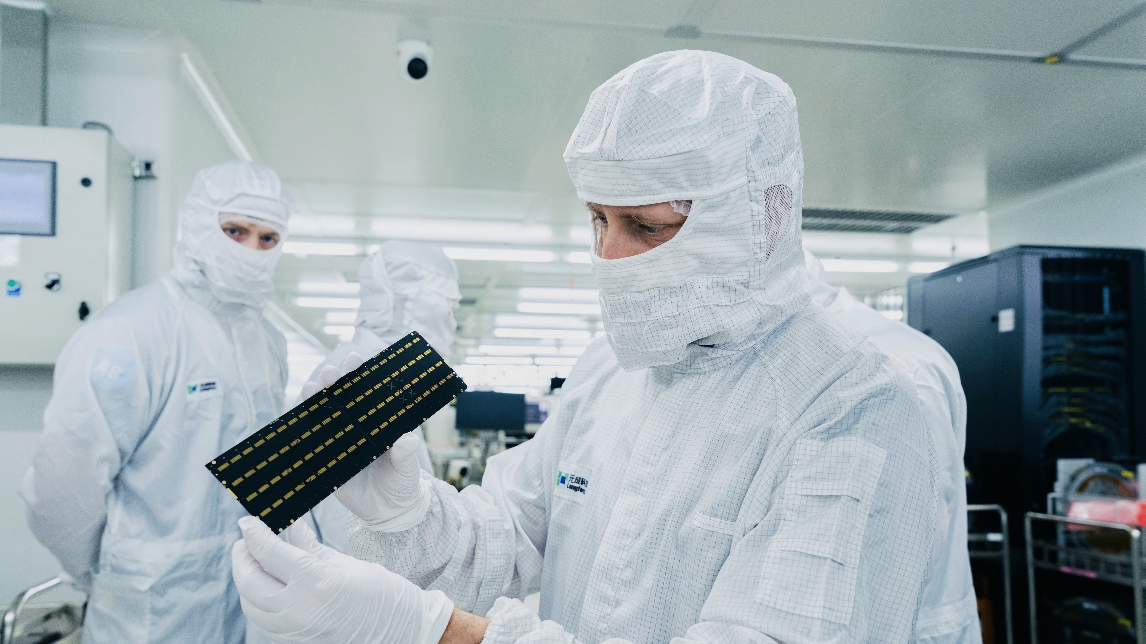
This photo below shows a container of cut and processed chips from that wafer.
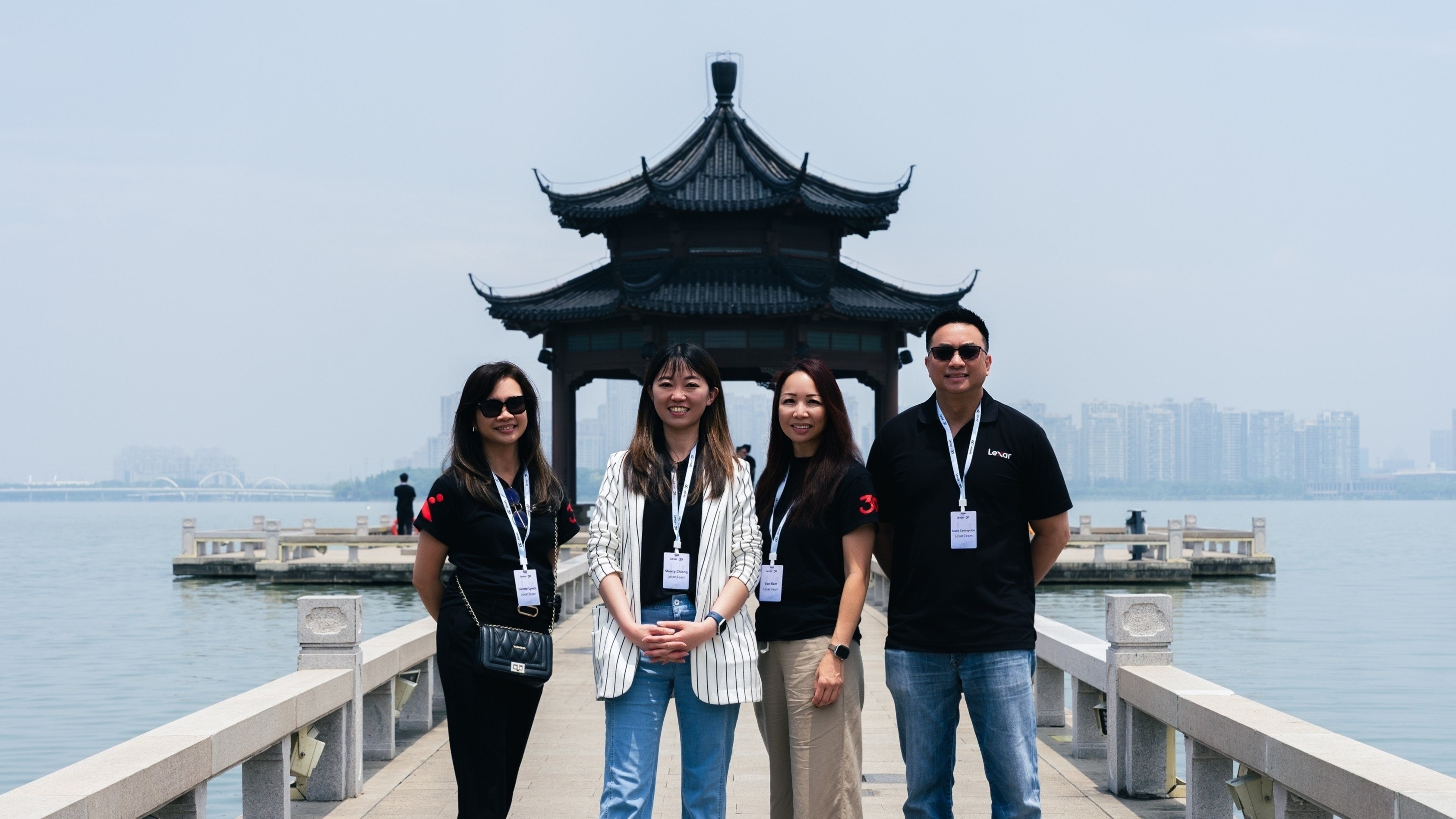
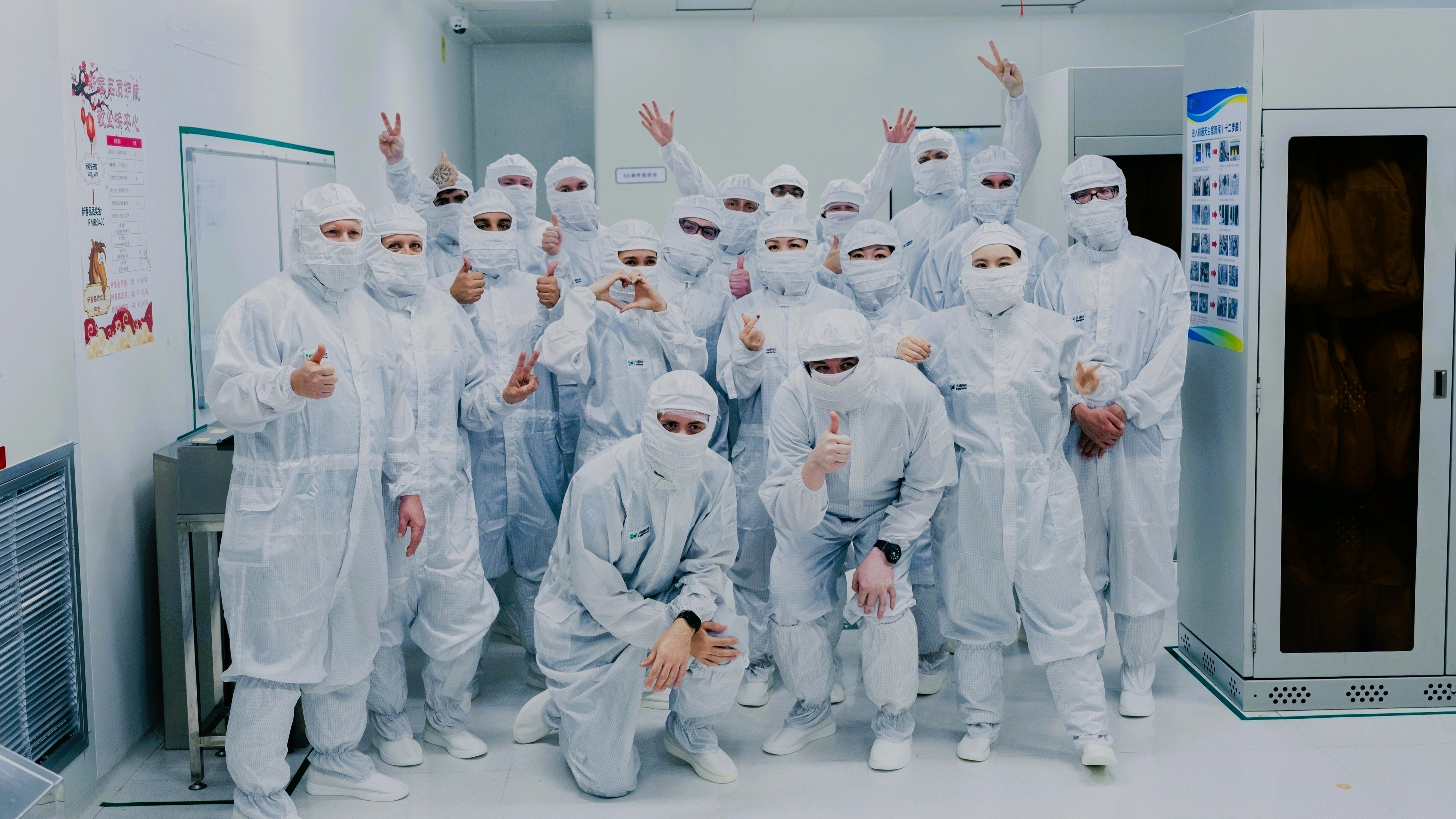
This photo depicts the US Lexar Team that took part in the planning and execution of this tour. From left to right, Lizette Lynch (North America Marketing Director), Sherry Chiang (Manager of Product Marketing), Van Baer (GM of Lexar North America) and Jason Concepcion (Senior Demand Planner).