
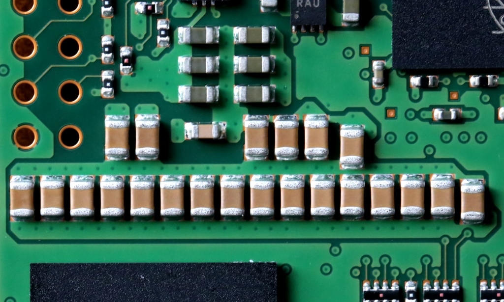
NAND FLASH MEMORY
NAND flash memory is where your data is stored (or retrieved from) and typical SSDs are made up of 8 or 16 modules, all SSD memory being non-volatile which means that constant power is not necessary to retain the data. SSDs consist of SLC (single-level cell). mlc (multi-level cell) or TLC triple-level cell) memory and the type will reflect, not only price, but the lifespan (or endurance) of the SSD.
SLC memory is extremely expensive and only seen in high end enterprise systems that require a memory endurance of 100,000 program/erase (P/E) cycles. A P/E ccycle can be seen as each time the SSD is filled and erased. Traditional MLC can be anywhere from 5-10,000 cycles with TLC coming in at 3,000 cycles endurance, although in more recent production we have seen 3,000 P/E cycle MLC with as little as 1000 P/E TLC memory. In spite of all of this, rest assured that the likelihood of a typical consumer SSD ever reaching end life is extremely remote. The lifespan of any SSD exceeds that of a hard drive significantly.
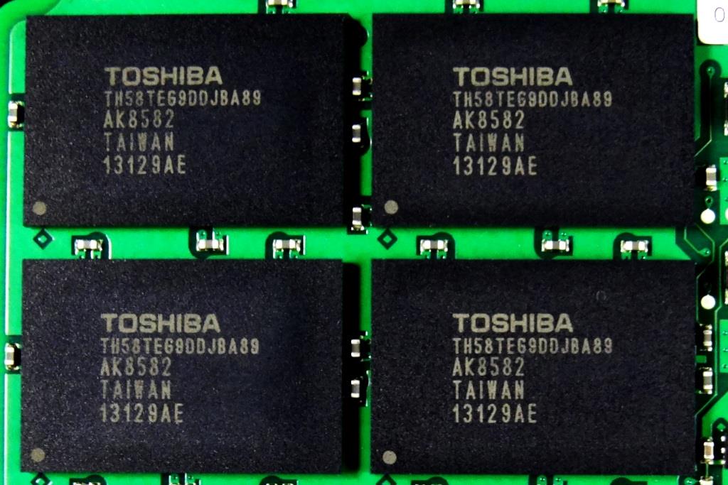
Many have recently heard the term ‘die’ with respect to memory and a die could be understood as being a single layer. There are typically 4 or 8 die in a stack and a 64Gb memory chip would be said to have 8 x 8Gb die packages, although Samsung has most recently used 16 die stacks providing for a 128Gb chip. Consider it similar to stacking 4 pallets of eggs and carrying them from one place to another, rather than carrying each pallet one at a time when we think of data storage and transmission. In their own way, die serve a similar purpose to channels.
Another important consideration of memory is that, at least at the retail level, capacities are of a standard value, these typically being 64, 128, 256, 512 and 1024GB. One may also see SSDs that are 60, 120, 240, 480 and 960GB and these SSDs contain 7% over provisioning which we will discuss in a later report. Briefly though, over provisioning provides for sustained performance and endurance of the SSD.
INTERFACE
The SSD interface is the architecture by which data travels in a specific hard drive or SSD and can be recognized in several cases by the connector that data cables are connected to on the SSD.
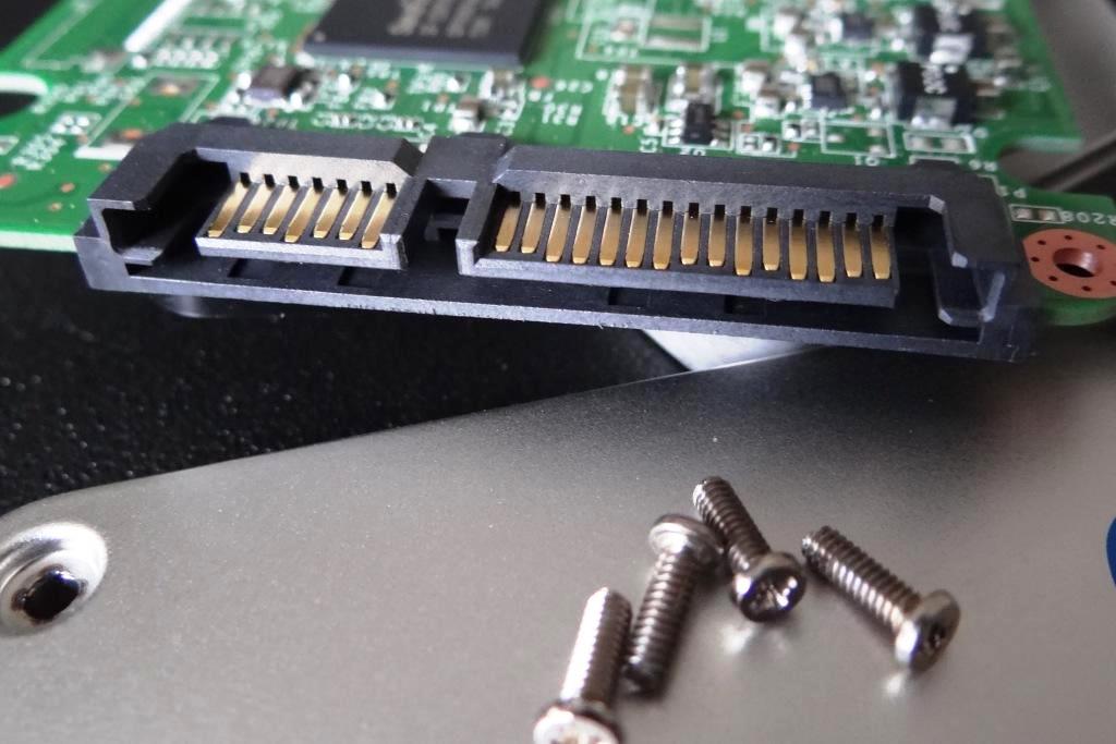
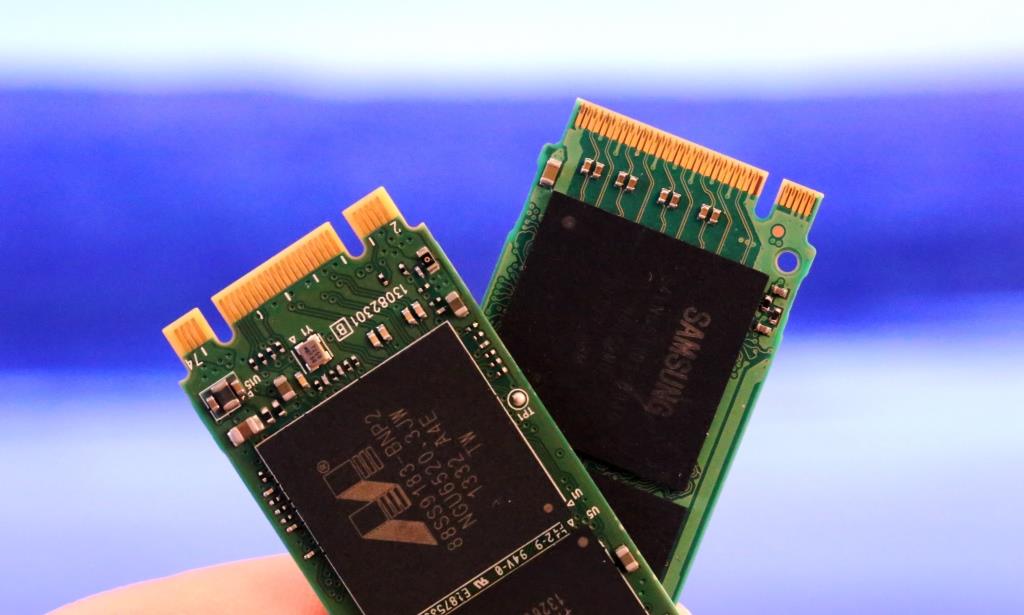
The interface will also play a vital role in data transfer speeds and a SATA 2 interface is capable of typical data transfer up to 275MB/s (ie. Solidata 2TB SSD Report), whereas a SATA 3 interface is capable of about 570MB/s (ie. Intel 730 SSD report) Newer M.2 SSDs have a PCIe 2.0 interface that can be two or four lanes. Two lanes (X2) increases that data transfer speeds up to 1GB/s theoretically (ie. Plextor M6e M.2 SSD Report) whereas 4 lanes (x4) can theoretically double that (ie. Samsung XP941 SSD Report).
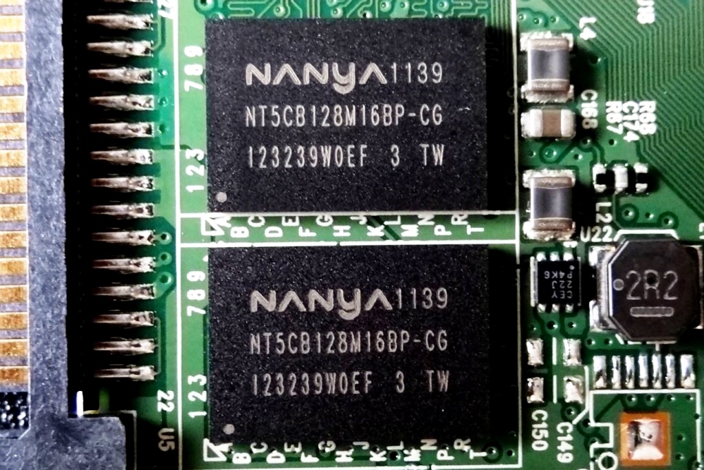
DRAM CACHE MEMORY
DRAM cache memory is becoming less common on SSDs, however, serves the purpose of increasing the speed that data travels from the controller to the memory significantly. SandForce based controllers, as well as custom-built Marvel controllers used by Toshiba, do not use a DRAM cache. In SSDs that use a DRAM cache, memory cannot be retained in the cache when there is no power to the SSD. The newest Crucial M550 uses a DRAM cache buffer and is the only retail SSD that also contains power capacitors, should the PC experience a power loss.
POWER CAPACITORS
Power capacitors provide for enough power to complete the data transfer operation from the cache to the memory in times of power loss. Have you ever simply shut down your PC only to realize that you never saved your work? Power capacitors limit data loss significantly and are very uncommon at the consumer SSD level with the Crucial M500/M550 SATA 3 SSD families being the first to offer this feature standard. ADATA has just also released their S920 and this SSD is also based on the M550 with power capacitors present.
PUTTING IT ALL TOGETHER
Data travels to an SSD through a cable attached to the SATA interface connector and then through the SSD controller where it is dispersed to memory for storage. Such things as the type of interface, number of channels the controller is capable of, DRAM cache and the amount of die in a single memory chip can increase the speed of that travel significantly. An interesting fact that displays how far advanced the controller really is might be the fact that firmware in the controller is capable of monitoring each cell of memory constantly in order to ensure that the memory wears evenly as data is stored.
Through this activity, the exact data storage location can be identified and, in fact, data is moved from one cell to another within storage constantly to ensure even memory wear levelling. If you consider a hard drive where the data is retained in the same location over time, this feature alone has the ability to reduce disk fragmentation significantly. We will dwell into this much deeper in future reports but thought this might be an ideal point to display just how amazing the SSD really is.
KEEP UP WITH THE ‘LEARNING TO RUN WITH FLASH’ SERIES!
- SLOW SSD TRANSITION AND THE CONSUMER MINDSET
- WHAT IS AN SSD?
- WHAT ROLE DO SSD COMPONENTS PLAY?
- HOW DOES AN SSD WORK?
- SSD THROUGHPUT, IOPS AND LATENCY EXPLAINED
Doesn’t the M500 also comes with power capacitors?
Yes…should have clarified the Crucial M5 series…
Very-very nice article Les 🙂
Another fantastic Article ! 🙂
One thing to add though;
> MLC can be anywhere from 5-10,000 cycles with the newest TLC coming in at 3,000 cycles endurance.
Although this was true in the 3xnm flash days (and to some extenet still is), flash today, manufactured at 20nm (or 19nm for samsung/tosh) is usually only rated for 1k/3k p/e (tlc vs mlc). Although one thing is true though; in most cases flash lasts much longer than its rated lifespan (some reports indicate up to 10x longer).
>There are typically 4 or 8 die in a stack and a 64Gb memory chip would be said to have 8 x 8Gb die packages.
There are also packages with 16 die stacks (mostly used in space constrained formats, such as msata — 1TB 840evo is a prime example of 16 stack die use).
Thank you Benjamin and I have added your points to the article! Perhaps you should consider writing one or two of the next eheheh.