
SK Hynix, Inc., a world-leading producer of NAND flash solutions, is announcing development of a UFS (Universal Flash Storage) 2.0 solution that is based on their own 16nm NAND Flash memory, as well as a proprietary controller and in-house firmware. This new UFS 2.0 solution offers a groundbreaking increase in performance, enabling the High-Speed Gear 3 Interface (up to 5.8 Gb/s) with dual data lanes.
 The UFS 2.0 standard is the next generation of embedded flash memory to eMMC for mobile devices, driving a significant boost in read and write speeds. UFS 2.0 also supports both low power and high density. SK Hynix’s UFS 2.0 solution operates at (up to) 780 MB/s sequential reads, and (up to) 160 MB/s sequential writes. It also offers random read speeds of (up to) 32,000 IOPS, and random write speeds of (up to) 17,000 IOPS. This represents three times the performance as compared to eMMC 5.1.
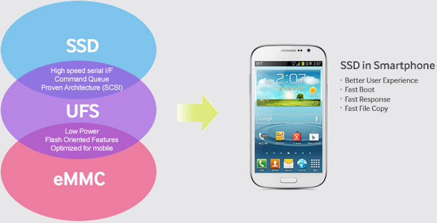 image source: androidauthority.net
According to Young Joon Choi, Senior Vice President at SK Hynix (and Head of their NAND Solution Development Division), “SK Hynix is pleased to expect the mobile devices such as smartphones to enhance their performance with the advanced UFS 2.0”.
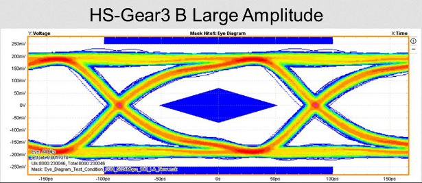 image source: blogs.synopsys.com
UFS 2.0 also utilizes ‘Command Queue’ technology, as is used in SSDs, to handle both read and write commands simultaneously. This improves data operation efficiency by preventing buffering during multi-tasking, and orders the priority of data operations. In order to maximize the command processing feature of the UFS standard, SK Hynix’s new device utilizes internal ‘Multi-Thread’ read processing to ensure that high-priority commands are processed first, regardless of other pending tasks. This delivers faster response for time-sensitive host requests, enabling the best user experience. As a result, superior performance in speed and power consumption is achieved as compared to eMMC.
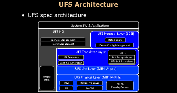 image source: mandetech.com
High-end smartphones are expected to have UFS installed beginning this year, and then gradually also migrate to the mid- and low-end devices. Industry analysts HIS Technology indicate that UFS is anticipated to have a 4% adoption share this year, and grow to 23% by the end of 2017, and to 49% by the end of 2019. You can view SK Hynix’s press release announcing their new 64GB UFS 2.0 solution in its entirety here.
![]()
Why do the even bother with another interface ?
Why dont SoC manufactureres and NAND makers move to pci-e entirely ?
You have much better speeds, much much better random performance and an already known interface.
Is eMMC/UFS less complex or uses less power ?
It is managed NAND meaning that it has the controller and interface built in. Overall, it is also a smaller design for mobile devices such as phones, tablets, GPS, etc. UFS is like the next gen of eMMC and both use less power than standard SSDs.
I suppose that makes sense.
But from a cost standpoint, it would make more sense to have onfi/toggle interface on the phones/tablet/etc pcb and let the SoC do the NAND managment. That way you have cheaper NAND and i suppose better selection on the market.