
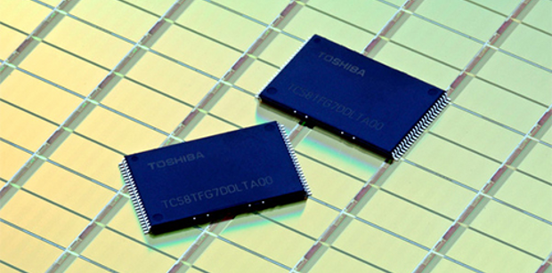
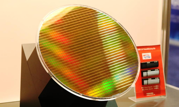
Toshiba Corporation is announcing development of the world’s first 15nm process technology for production of NAND flash memory. Toshiba will begin mass production of two-bits-per-cell, 128Gb (16GB) NAND modules at the end of April 2014 at its Fab 5 Yokkaichi Operations, which is Toshiba’s primary NAND flash production facility. The new 15nm process replaces Toshiba’s second generation 19nm process technology, which had been their previous flagship NAND.
Toshiba is also applying the new 15nm process technology to three-bits-per-cell NAND, and anticipates beginning mass production in June of 2014. The three-bits-per-cell 15nm NAND will also be produced at Fab 5, where this “stage two” is currently under construction. Toshiba will also be concurrently developing controllers for embedded NAND flash memory, and will introduce three-bits-per-cell chips for tablets, smartphones and other mobile devices. They will eventually extend product applications to notebook PCs by developing their own controller that is compliant with solid state drives (SSDs).
Toshiba has now achieved the world’s smallest class of chip size via the 15nm process technology, and has also developed improvements in their peripheral circuitry technology. The new 15nm chips attain the same write speeds as their previous 19nm process technology, while boosting the data transfer rate to 533 MB/s; which is 1.3 times faster than previous chips. This is achieved by utilizing a new higher-speed interface.
Toshiba will continue to execute its process technology development roadmap, strengthening its performance and product competitiveness by applying cutting-edge processes to production. Going forward, Toshiba will solidify its market leadership position by promoting ongoing product innovation and development, and ensuring that it responds to a broad range of client products; including tablets, smartphones and slim notebook PCs. These same philosophies will also be applied to enterprise products requiring high reliability, such as SSDs for datacenters.
![]()
The Toshiba press release on the new 15nm process technology can be viewed in its entirety here.
I wonder what endurance will be like (especially on TLC parts).If they can keep the ~1000 p/e, this will be pretty sweet for entery level ssd.
200€/1TB SSD anyone 🙂
Yeah, the prolific proliferation of these TLC products also has me wondering about endurance , but I guess since most people upgrade smartphones and tablets (for new) every other year it may not be an issue …… but people who buy second hand devices may be in for a nasty shock !
Even if it only had 500 p/e, its still more than enough for an avarage user…
Just check your writes if you have ssd and you’ll see 🙂
Thos news about 15nm sounds great but I am disappointed to hear nothing about using it for SLC …
Is Toshiba phasing out toggle NAND? Can it even exist in a 3-bit scenario?