
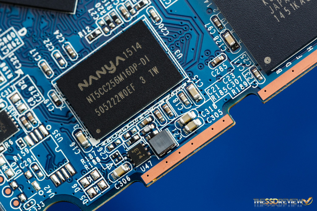
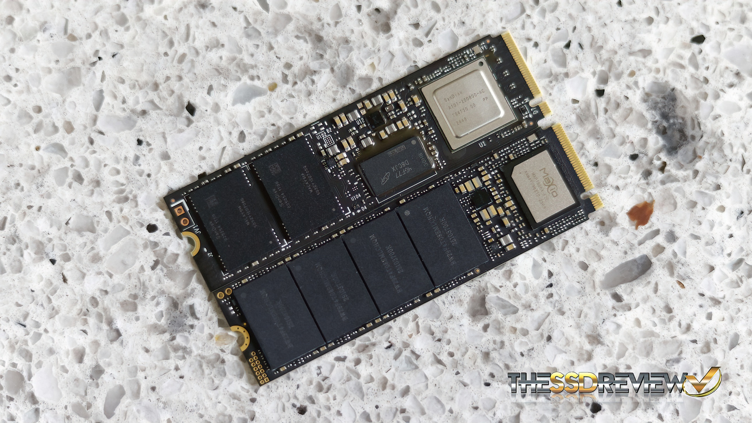
After NAND Flash and controller, DRAM is perhaps the most important component on an SSD. In our premier article of our newest ‘ Learning to Run with Flash 2.0’ entitled, ‘Understanding SLC, MLC, TLC and QLC NAND Flash‘ we provided an understanding of the different types of NAND and value of each in the SSD spectrum. Today, we’ll be taking a step further and discussing DRAM vs DRAM-less SSD designs. DRAM in SSDs serves many roles, the most important being the storing and managing of data structures, such as the Flash Translation Layer (FTL). Sounds confusing right? Follow along and we will make things simple.
Consider the FTL similar to an Index in a book that enables you to get to a chapter very quickly. FTL maps the logical block address (used by operating systems) to physical locations on the NAND flash. In simple terms, it is a mapping table that keeps track of where specific data is located on that NAND. DRAM ensures the controller has fast access to this table, allowing it to locate the data quickly whenever required. Additionally, DRAM on an SSD serves as a high-speed data buffer, helping to reduce latency and enhance overall NAND flash performance.
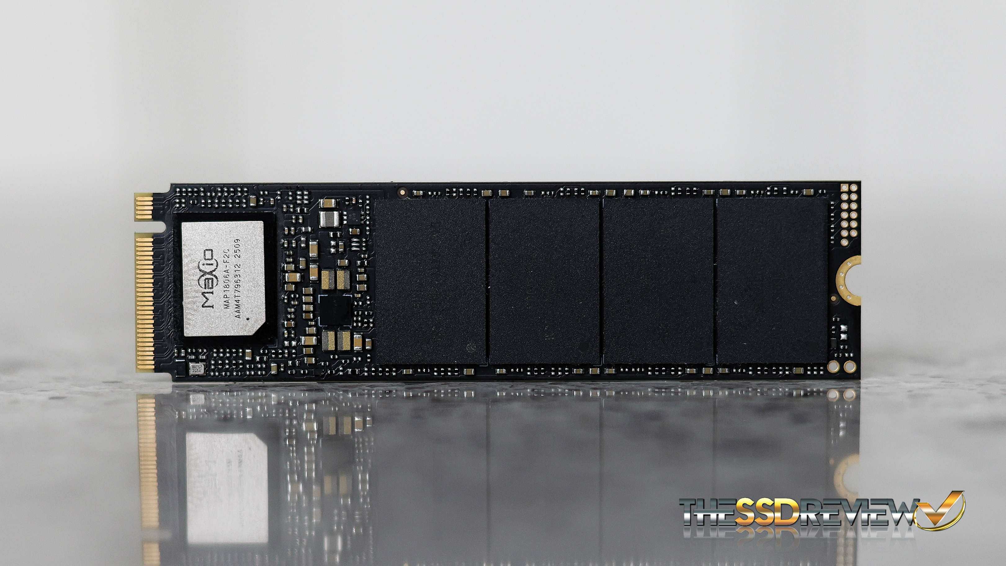
DRAM is a beneficial component of SSDs, but is no longer necessary since Windows 10, in fact, when HMB came into play. Today, SSDs can utilize the system’s RAM as a Host Memory Buffer, or HMB. SSDs that use HMB rather than a physical DRAM chip are known as DRAMless SSDs. These designs are typically implemented on budget drives.
Instead of the on-chip DRAM, the controller and operating systems divide some space from the system’s main memory and assign it as an HMB. There are some drawbacks of DRAM-less SSDs, such as higher latency and slower read speed. In this article, we will speak to issues relating to DRAM-less SSDs and why they can sometimes be a good option. Let’s start by understanding the purpose of DRAM (Dynamic Random Access Memory).
WHAT IS THE PURPOSE OF DRAM IN AN SSD?
DRAM is a high-speed cache or buffer between the host system and the NAND flash. As DRAM has very low latency and very high raw read/write speed compared to NAND flash, it is perfect for handling the incoming heavy streams of data. This accumulated data can then be stored in the permanent NAND in the background. In order to work together with the host, the mapping tables must be quickly accessed and re-updated. DRAM, with its high raw read/write speed, helps the controller have access to the FTL.
UNDERSTANDING THE FILE TRANSLATION LAYER (FTL)
NAND can not be written to an SSD directly. It must be erased at the block level and then written at the page level. The NAND programming model mandates that a page can only be written once it has been erased. If a page is partially filled and we need to update it, the new data cannot be written to the same page; instead, the updated data must be written to a new, clean page, and the old page is marked as invalid. This process is managed by the Flash Translation Layer (FTL).

On the other hand, the operating system expects a linear array of Logical Block Addresses. It also expects a simple data structure like a list of blocks 0, 1, 2, and so on. NAND Flash is fundamentally incompatible with this way of data reading and writing. The flash translation layer (or index) assists the OS in utilizing NAND flash with its own method of data organization.
FTL acts as a real-time translator. It makes the NAND flash appear as a normal overwrite-capable and random-address block device. A significant amount of code runs in the background with processes like mapping tables being created and updated, garbage collection, write redirection, and wear leveling. A 1TB SSD would normally require 1 million 4KB logical blocks with hundreds of megabytes of metadata. To access, create, update, and delete this metadata, DRAM serves an important role and hence makes our SSDs faster.
HOW ELSE DO DRAM BENEFIT SSDS?
SSD DRAM plays a major role in write buffering. Write buffering is the process where newly introduced data is temporarily held in a buffer before its final physical write to its storage location. As a result of SSD ‘erase-before-write’ restrictions, DRAM acts as a write cache and handles the incoming bursts of data temporarily with its high read/write speed.
DRAM and RAM are volatile, meaning that the information is lost once the power is removed. SSDs are brilliant with their ‘journal commits’ and capacitors that prevent data loss if a power failure occurs. In these instances, if the system loses power, the data still in the DRAM is moved to the NAND flash for permanent storage. The next time the system is booted, that information is loaded back into the DRAM.
DRAM also helps with data prefetching, which improves the read speed, as well as garbage collection and heap-leveling by allowing faster map access. All the algorithms generally run in the background when the SSD is idle, which means, with DRAM access, these background processes have little to no impact on SSD performance.
HOW DO DRAMLESS SSDS WORK?
SSDs can function perfectly without any onboard DRAM or HMB by storing their mapping tables directly in NAND Flash. This was common in most SSDs before 2014, especially in lower-cost models, however, accessing these tables from NAND is slower and less efficient than using DRAM. Host Memory Buffer was introduced in 2014 with the release of NVMe 1.2. It began to get adopted in consumer SSDs between 2015 to 2017. Today, nearly all DRAM-less SSDs rely on HMB, so our discussion will focus on DRAM-less SSDs that use the HMB mechanism.
BORROWING A CHUNK OF DRAM FROM THE HOST SYSTEM
In DRAM-Less SSDs, SSDs temporarily use a small part of the computer’s main memory (RAM) and use it as a replacement for DRAM. This request is sent through the NVMe protocol just when the system boots. This portion is always shared during a fresh boot and when the system shuts down, the data on the DRAM is saved in the NAND flash for permanent storage. This process happens again in the next boot.
The SSD’s built-in software (called firmware) works with the operating system to set everything up through the NVMe driver. The size of acquired RAM is generally dynamic and varies based on the capacity of the drive and the task at hand.
Once the system grants access to this memory, it is no longer available for the system. This access is given via the PCIe bus using Direct Memory Access or DMA. DMA allows the SSD to read and write data to and from the host memory without much interference from the CPU. Imagine it as a bypass to the DRAM. The same type of data, like FTL mapping tables, write buffer, read cache, and other metadata, is stored in the HMB, but its location changes.
MAJOR DRAWBACKS OF DRAM-LESS/HMB DESIGN
As compared to the Onboard RAM, HMB is slower. This makes the DRAM-less SSDs slower by design in certain tasks. The key drawbacks are higher latency, slower performance in random read/write tasks, and increased write amplification. DRAM-Less SSDs also have less consistent performance during sustained use.
Even though PCIe lanes are fast and the latest advancements in HMB are amazing, the additional steps and the increased distance between the system RAM and NAND reduce the access speed and increase the latency. The impacts can be seen mainly in high IOPS tasks. HMB allows a limited memory size compared to what the manufacturers give on the onboard DRAM chips.
You might think, why don’t we tweak the firmware and use more of the system memory as HMB? That isn’t possible without the willingness of the host system and NVMe specifications. Also, the size of HMB doesn’t always help, especially when low latency and high DRAM performance are required to get things done. The small size of HMB often results in lesser performance when we work with large amounts of data.
I have the Kingston A400 in my old laptop, and it works just fine when I am doing anything casual. In mixed or heavy workloads like when I am running a virtual machine or compiling large codebases, I can clearly observe the difference when compared to my main system with a DRAM based SSD. The usual performance impacts are dropped IOPS and increased latency.
Excellent overview of this obscure implementation. Thank you for your contribution.
(Someone should proofread the final paragraph! ?)