
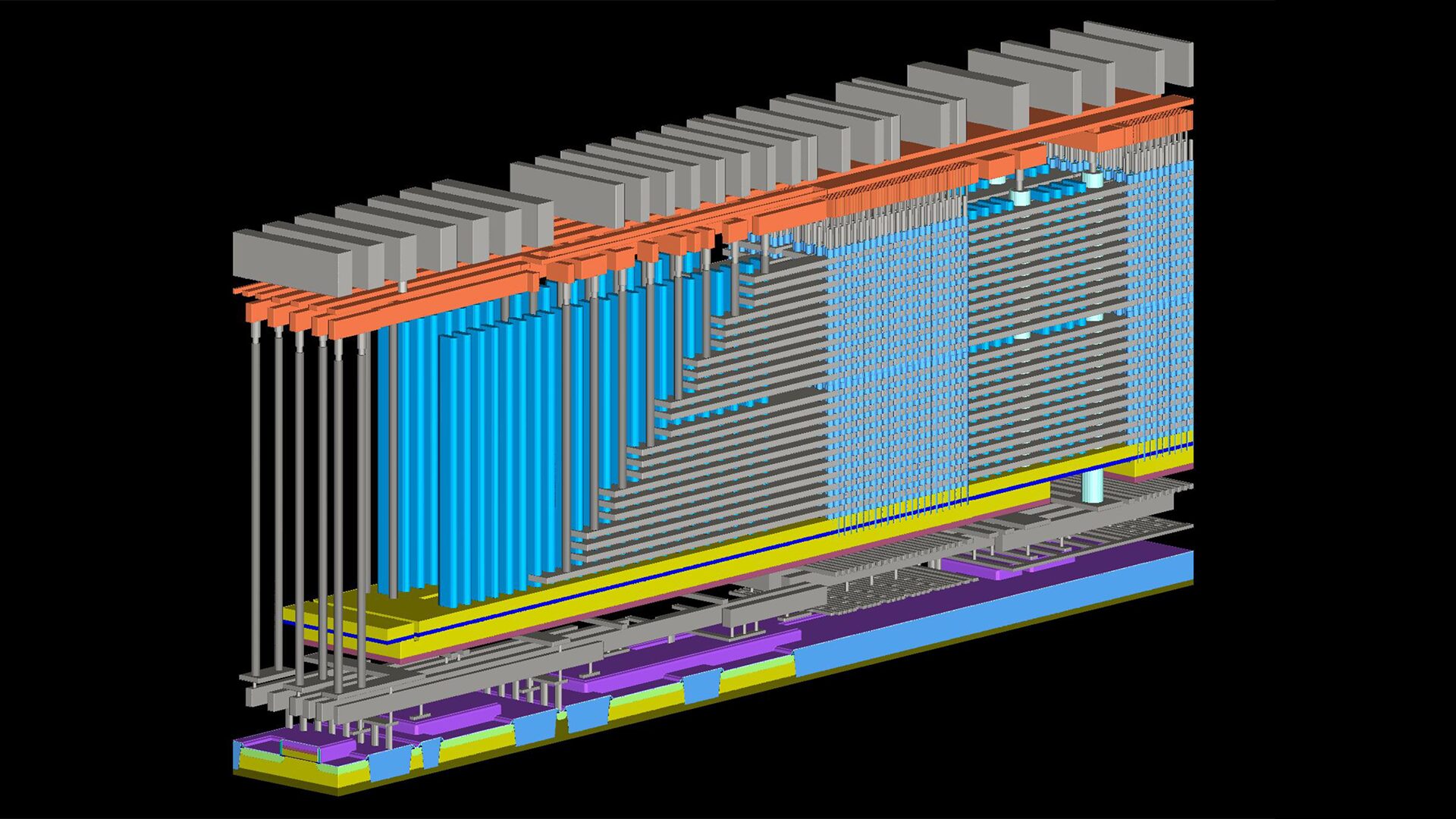
Explaining enterprise, data center and the newest AI-centric focussed SSDs can sometimes be a bit confusing to many but this week at FMS 2025, KIOXIA displayed something that I have tried to explain for years with respect to what exactly we do and how flash media is structured. Describing ‘flash’ is actually very simple, in that, it is like an apartment block with elevators. In the case of KIOXIA’s newest BiCS 8 3D TLC NAND it has 218-layers as an apartment might have 218 floors, and each layer has electronic connects as an apartment might have elevators. This explains how this is ‘3D’ memory and that apartment block looks something like this:
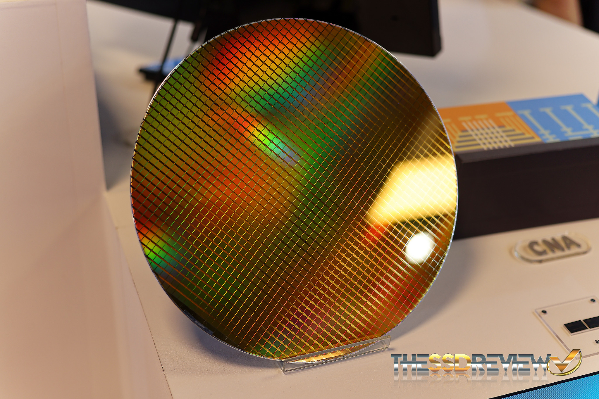
What is really incredible, at least in my mind, is that this chip started as one of these squares on this KIOXIA BiCS 8 NAND wafer, a shot we took at the KIOXIA Display at Computex Taipei earlier this year.
But whats even more incredible is how technology is able to create these 218-layers in a NAND flash memory chip that is only millimeters thick as we can see here.
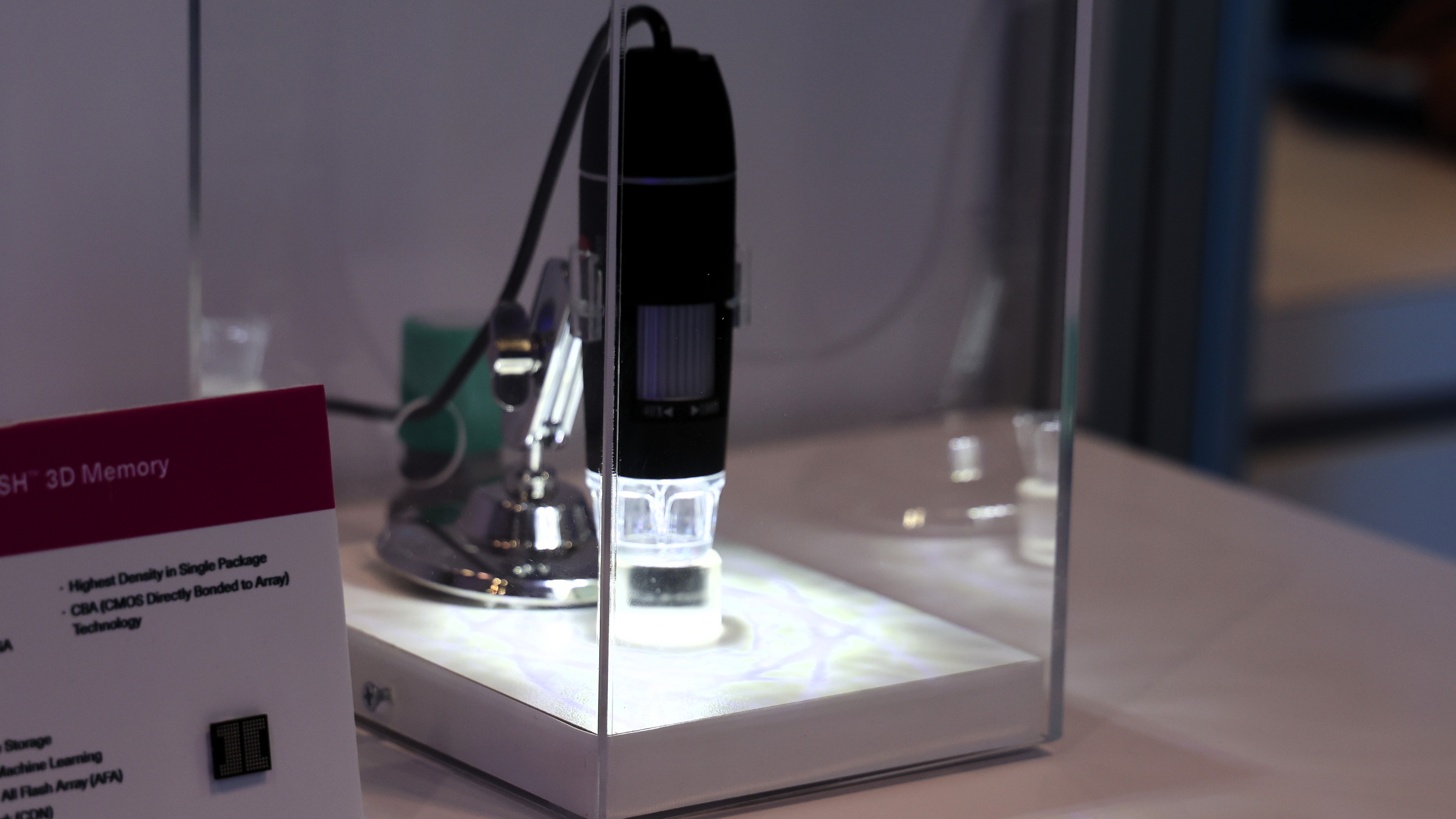
Something we have never been able to do before today, however, is to visuallize this through an actual picture. Take a look at this shot of the BiCS 8 QLC 32-die stack through a 1000x endoscope and we can now actually see layering.
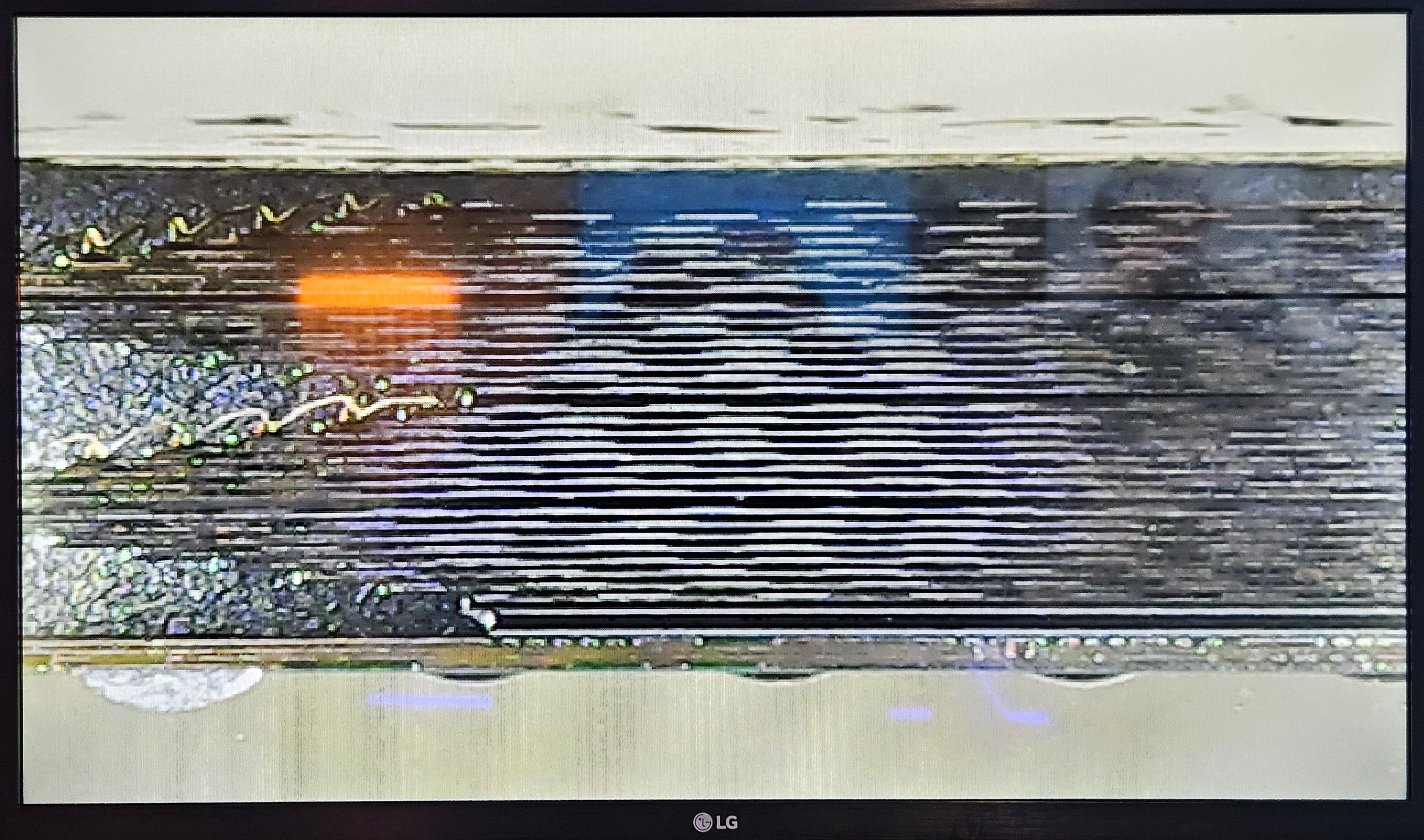
Yes… I may be a bit of a geek at times but I am in awe of this shot. It’s not so much the layering as it is the fact that this, or rather chips that resemble this same process, our in our hands and used by us every day of the week… and we don’t even know it. This is the beginning of what we no consider an ‘instant’ everything world… Thank you very much for this KIOXIA!
This video does a great job of visualizing all that I have tried to explain, taking things a step further by explaining CBA Technology with respect to its implementation in BiCS 8 as well…