
EXTREME ULTRAVIOLET LITHOGRAPHY TOOL
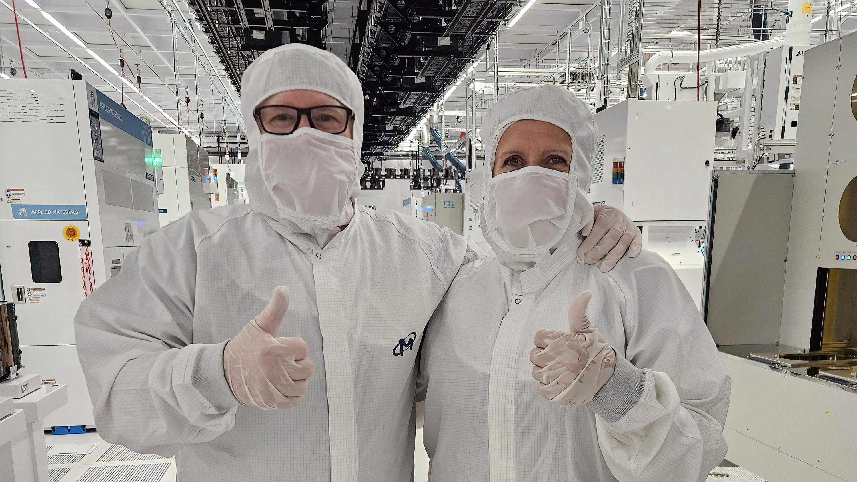
The ASML EUV is the meat and gravy of the Micron fab and photography was strictly forbidden. Fortunately, stock photos and videos were available to assist. This ‘tool’ is the size of a school bus, weighs 20 tons and took three 747 jets and 12 semi-trucks to transport to the Micron fab. It contains 100,000 parts, costs somewhere in the area of $250 million, and is easily the single most technical device ever created.
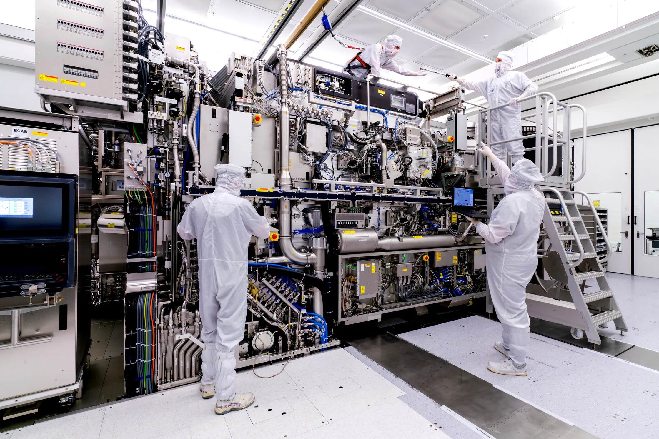
Its sole purpose is to etch extremely small intricate patterns onto the silicon wafer using short wavelength ultraviolet light. There is no discussing this machine without an understanding that it pushes Moore’s law forward which is the principle that the ‘speed and capability of computers can be expected to double every two years, as a result of increases in the number of transistors a microchip can contain’.
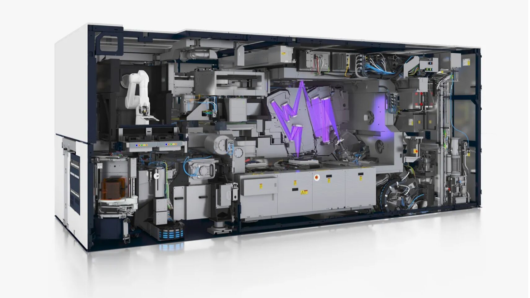
In short, a powerful laser within the EUV fires on microscopic droplets of molten tin which turn it into plasma and emit extreme ultraviolet light. This light is then focused into a beam and reflected off several surfaces which contain the intricate design of the circuitry of the desired microchip. This pattern is then etched into the cast of the silicon wafer at a microscopic level. I am afraid that explanation may be a bit basic but ASML has just released a very easily understandable video explaining EUV technology which can be followed here:
So when will we see the beauty of the EUV first hand? Micron’s newest 1y (1-gamma) DRAM is built using the EUV Tool. The end result is the newest 1y 16GB DDR5 memory with up to 9200MT/s speeds, 30% improved memory density per wafer, 20% better power efficiency and a 15% performance boost from the former 1y (1-beta).
I don’t follow stock but Micron Stock has doubled since the big dip of April this year and sits at 128.89 as of the writing of this report, a jump of 53% for the year to date. Micron has made some very wise moves with its investment of $200 billion as we spoke of earlier in this report. Not only are is there a fab under construction with another in the planning stage in Boise Idaho, but an environmental review is presently being conducted for another in Clay, New York, for what is sure to be the one of the world’s largest and most advanced memory fabrication facilities. This photo is the projected facility which is subject to change.

The facility will house four ‘clean-room’ fabs at 600,000 square feet each, much the same as the new fab being built in Boise that will begin wafer output in 2027. It will also house 290,000 square feet of clean-room support space and 250,000 of administrative space. Micron projects 9,000 direct Micron jobs and 40,000 community jobs in New York. The number of total direct and indirect jobs projected for all Micron expansions is 90,000.

REPORT SUMMARY AND FINAL THOUGHTS
Our initial invitation to Micron was rather unexpected. The access granted that enabled this report few get the opportunity to experience. We would like to thank Micron for this opportunity and hope that we were able to put together a product that helped you understand technology, and more specifically the wonders of flash, just a bit more.
Now…look at your smartphone. Before reading this report most knew nothing of the inner workings and the truly amazing technology within. We spoke of Moore’s law which is a direct correlation as to why that smartphone in your hand today is much more powerful than your PC of not so long ago.
 This report touches every piece of electronics we see each and every day. Thank you for taking the time to follow along! Last but not least, check out this newly published Micron video which provides a closeup look and one of the United States largest construction endeavors.