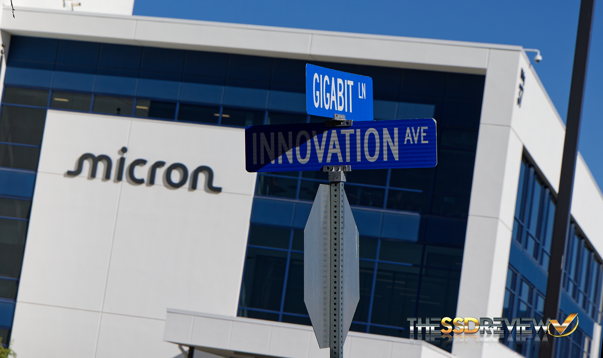
On approach to Micron Headquarters, there is no doubt at all that you are entering a flash memory manufacturing facility with roads named Technology Lane, Memory Park Lane, Terabyte Lane, Data Drive and, in recognition of Micron’s former CEO Steve Appleton, there is S Appleton Drive.
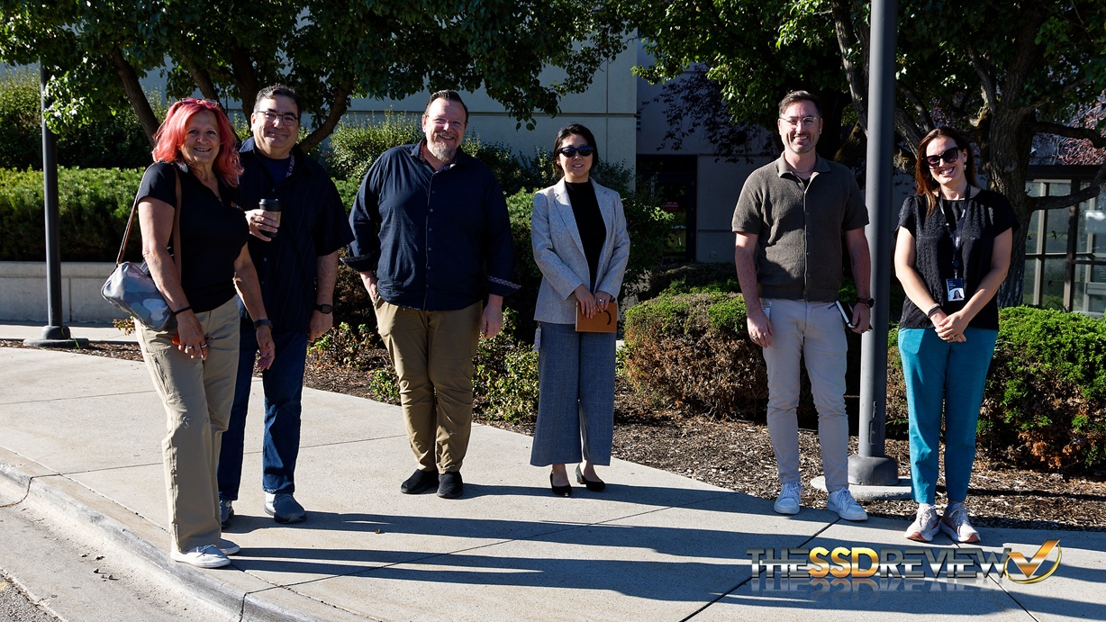
Next up…the team. We were fortunate to be accompanied by some new, along with a few longstanding friends that we had known in the SSD industry for some 13 plus years. From left to right, Karen Tokar (TSSDR CEO), Jonathan Tanguy (Micron Principle SSD Product Engineer), Jonathan Weech (Micron Sr. Director of Product Marketing and Management), Mengxi Liu Evensen (Micron Director of Product and Technology Communications), Mark Welch (GOLIN Senior Vice President and Executive Director), along with Katie Terhune (Micron Internal Communications Manager).
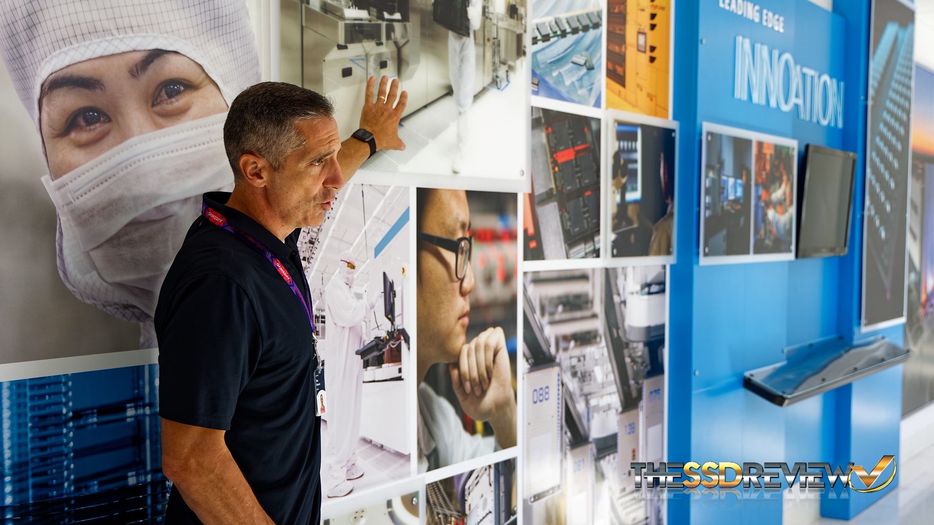
To start our tour, meet our tour guide Ren Hansen. Ren has been with Micron for 30 years and his present position is that of Project Manager of Micron Fab 4 TD Operations. A great part of his Micron service has also been as a Hiring Manager, and right away one could tell Ren knew people. His explanation of very technical things as we moved through the tour provided a fluent understanding by all.
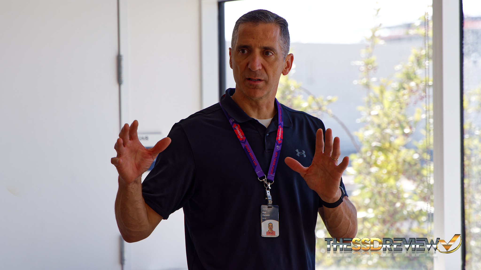
One could tell they were in for a treat with one of Ren’s initial statements, “We are pretty awesome”. Even better though was Ren’s metaphorical description of a silicon wafer’s development as being similar to that of perfecting a cookie recipe. He described creating the perfect cookie as having 10-12 steps, a solid recipe and taking 45 minutes where you want to consider tweaking things to make them better.
In comparison, the Micron recipe for creating a wafer was called ‘The Traveller’, contained 1600 steps and each wafer takes 2-3 months while constantly tweaking the recipe. New tools or processes may be introduced which may only effect a certain number of the steps, always ‘taste testing’ as they build and tweak the final product. Any discarded wafers are recycled and the end goal is wafer production in and around six weeks.
IS IT A FAB AND/OR FOUNDRY?
Wafer fabs and wafer suppliers serve two different functions with respect to flash chip development. A silicon wafer supplier manufactures or “grows” silicon ingots through a process of gathering large amounts of sand (some from Canada in the case of one of Micron’s suppliers, Shin-Etsu of Japan) where it is essentially turned into liquid glass through temperatures that achieve a melting point of 1700°C (3092°F). Once hardened, these ingots are then sliced into very thin wafers that serve as the basis for building the memory chips. Ren provides a great description of the process in this video:
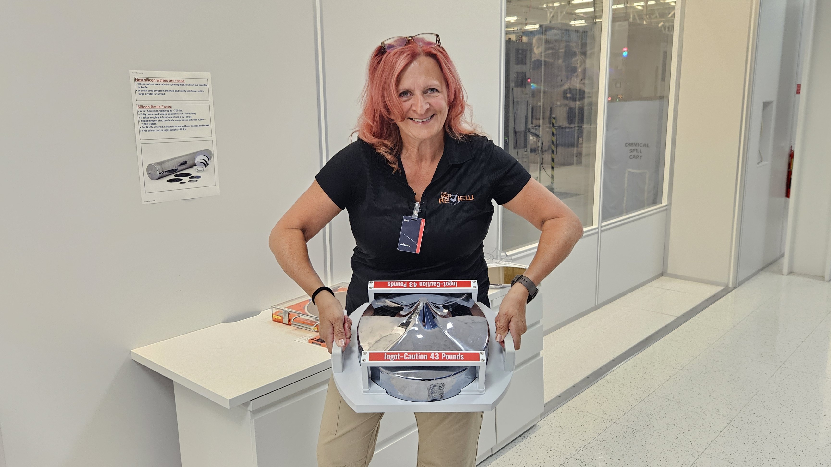
Micron’s public displays were beyond reproach and here we can see Karen handling the 43lb ingot top Ren was describing. A full ingot weighs approximately 700lbs, is 6-7ft in length and will produce 1500-2000 wafers. These wafers are one of the purest substances on earth being 99.9999999% pure compared to a diamond which is 99.95% pure.
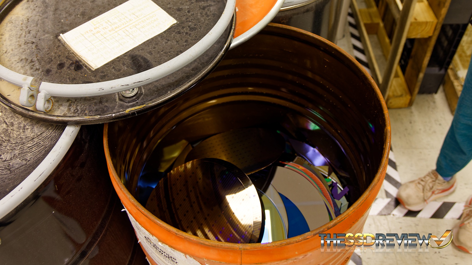
In the case of Micron Technology, bare silicon wafers are received by the factory pre-cut and tested and ready to be processed. New wafers arrive in mylar bags as they cannot be exposed to bare sunlight. Post processing, there are wafers that may not have progressed through all 1600 stages of development.
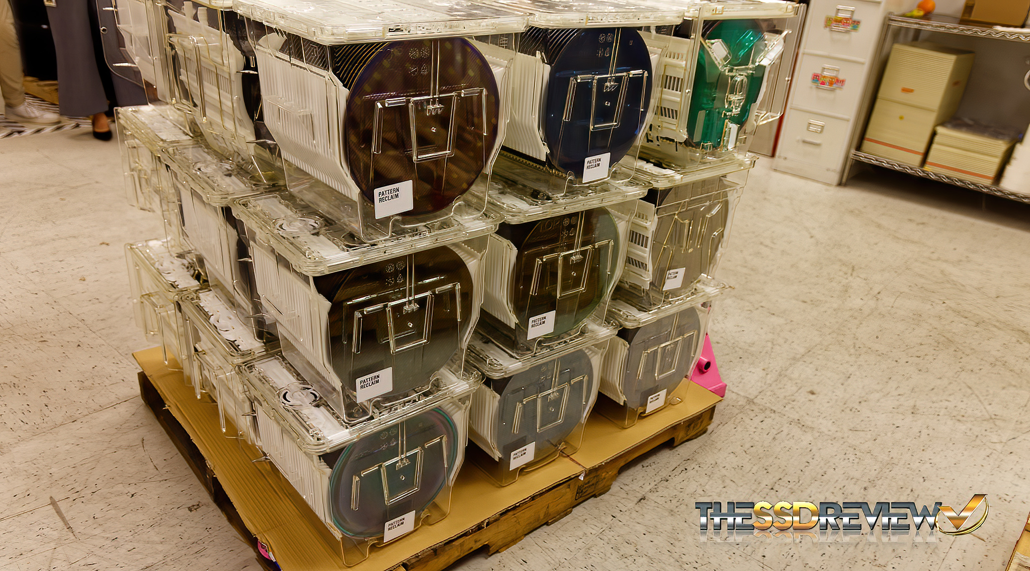
These are returned to the vendor, recycled or reclaimed and returned to their original state for reuse. This photo is from the recycle room which depicts 9 different rows of wafers each identifiable by different colors as having been refused at different stages of processing. Some are not fit for reclamation and are destroyed.
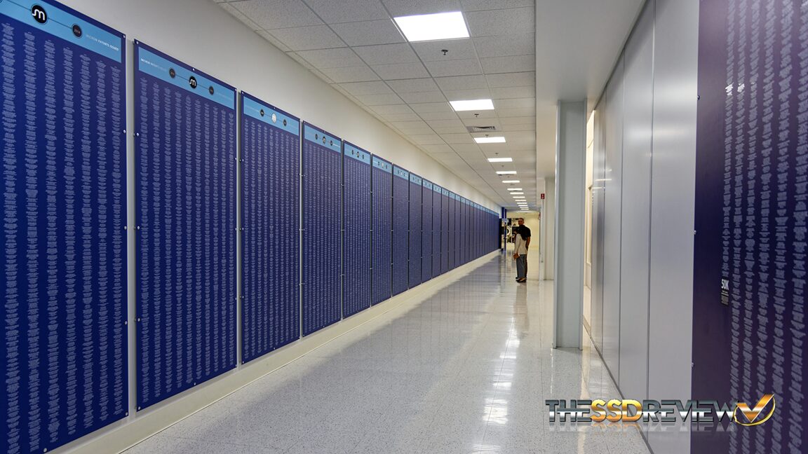
MICRON PATENTS AND A BIG SURPRISE
As a final touch to our public portion of the tour, we were shown Micron’s wall of patents. Micron’s first patent was in 1984 and to date they have almost 60,000 patents. Their primary patent holder is Micron’s own Dr. Gurtej S. Sandhu who holds 1,280 patents, more than Thomas Edison himself. He is also one of the top ten patent holders in the world.
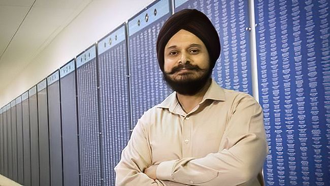
This photo was borrowed from Darpan Magazine which contains an amazing article entitled: Meet the Biggest South Asian Inventor in the World: Dr. Gurtej Sandhu. While examining the patent wall, we were surprised to learn that one of our own team was included in two patents which were not posted yet.
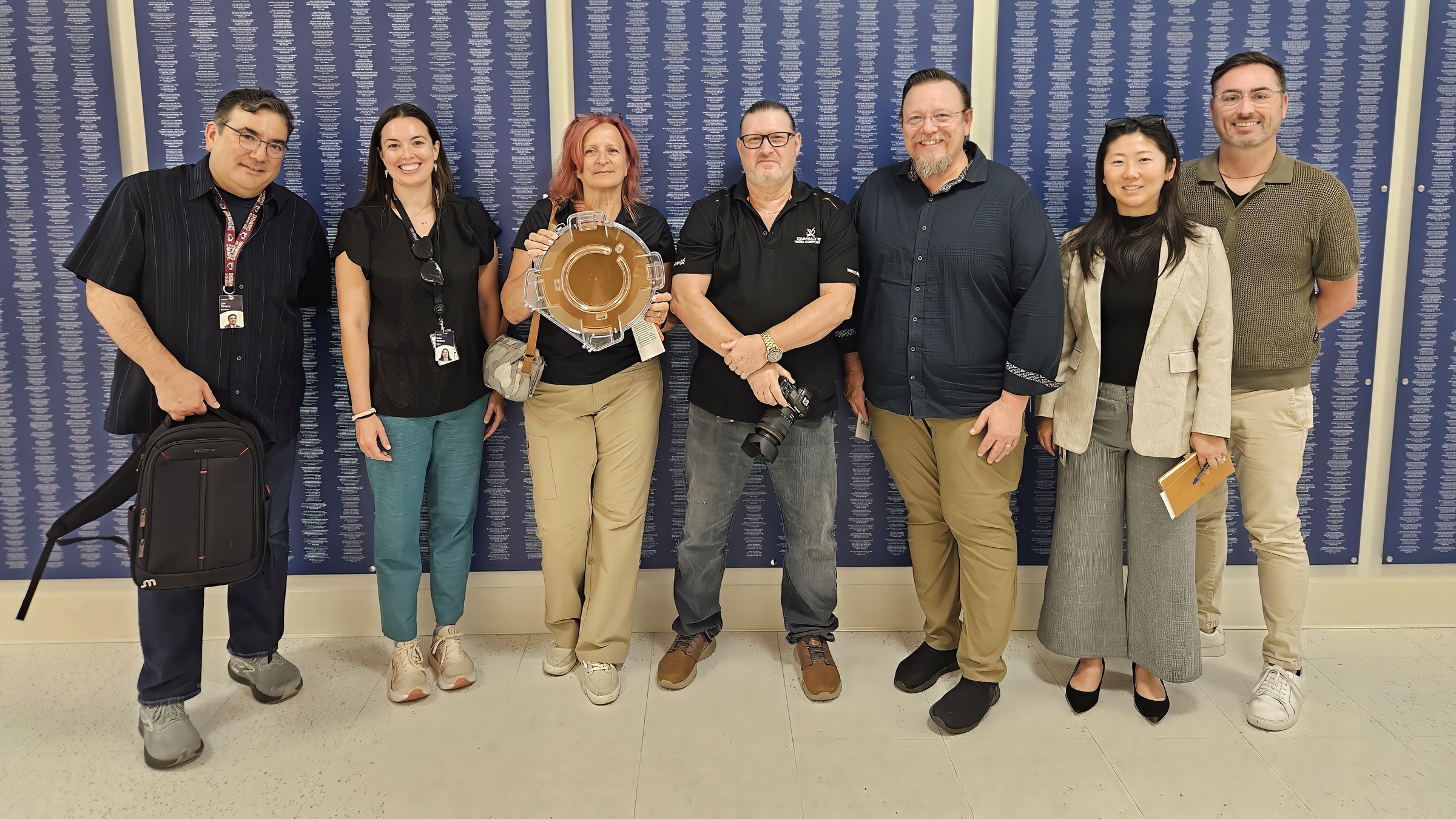
Jonathan Tanguy is to the left in the above photo and has been acknowledged as an Inventor for US Patent #10,854,299 B2 pertaining to Data Erase Operations for a Memory System, as well as US Patent #10,452,532 B2 for Directed Sanitation of Memory. Information on both patents can be found here.