
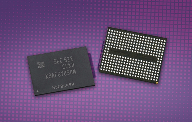
Samsung Electronics Co., Ltd., a world-leading producer of advanced memory technology devices, is announcing that it has begun mass production of the industry’s first 256-gigabit three-dimensional (3D) Vertical NAND (V-NAND) flash memory. This 3D V-NAND is based on 48 layers of 3-bit multi-level cell (MLC) arrays for use in solid-state drives (SSDs).
 Samsung’s new 256Gb 3D V-NAND flash has double the density of conventional 128Gb NAND chips. Along with enabling 32GB of memory capacity on a single die, the new 256Gb 3D V-NAND will easily double the density of Samsung’s current SSD line-ups, and is an ideal path for creating multi-terabyte SSDs.
 According to Young-Hyun Jun, President of Samsung Electronics’ Memory Business, “With the introduction of our 3rd generation V-NAND flash memory to the global market, we can now provide the best advanced memory solutions, with even higher efficiency based on improved performance, power utilization and manufacturing productivity, thereby accelerating growth of the high-performance and the high-density SSD markets. By making full use of Samsung V-NAND’s excellent features, we will expand our premium-level business in the enterprise and data center market segments, as well as in the consumer market, while continuing to strengthen our strategic SSD focus.”
 Each cell in the new V-NAND chips utilizes the same 3D Charge Trap Flash (CTF) structure, with cell arrays stacked vertically to form a 48-storied construction that is electrically connected through approximately 1.8 billion channel holes that are punched through the arrays by utilizing a special etching technology. Each chip contains over 85.3 billion cells in total. They are able to store 3 bits of data each, resulting in a total of 256 billion bits of data – all on a chip no larger than a finger tip.
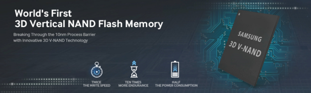 Using a 48-layer 3-bit MLC 256Gb V-NAND flash chip results in a power consumption reduction of over 30% as compared to previous 32-layer 3-bit MLC, 128Gb V-NAND chips (when storing the same amount of data). While for the most part utilizing existing equipment, the new chip achieves approximately 40% more productivity during production versus the 32-layer predecessor chips.
 Samsung introduced its 2nd generation of 3D V-NAND (32-layer 3-bit MLC V-NAND) last August, and continues to lead the era of 3D memory by creating a 48-layer 3-bit MLC V-NAND chip in just one year. Samsung intends to produce this 3rd generation V-NAND throughout the remainder of 2015, which will enable more accelerated adoption of terabyte-level SSDs. With the ability to now introduce consumer SSDs of 2TB and above. Samsung also plans to increase its high-density SSD sales to enterprise and data center market segments with leading-edge PCIe NVMe and SAS interfaces.
![]()